Update # 1
Im going to try and make this readable so bare with me. I broke it into parts for better understanding, i rewrote this like 4 times. I’ve decided until I iron out all of the kinks I wont be posting anything to github, Sorry for that.
So heres what I’ve got so far.
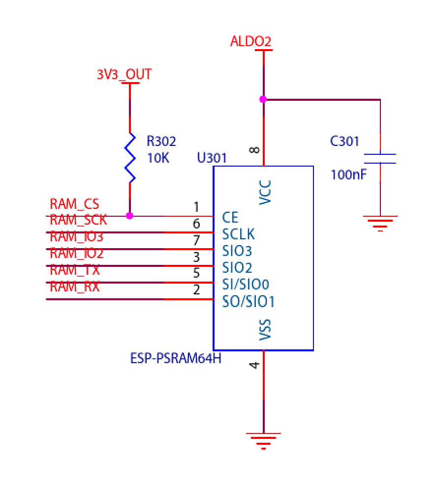
The first test was with the PSRAM,
- CS_PIN = Chip Select, high means it enables and low is disable.
- SPI OPEN 1000000, 0, 8, 5, 6, 7 1mhz, Mode 0, transfer size, SCK, MOSI & MISO pins. Since picomite cant use the hardware SPI on the gp pins, it bit-bangs them in the program.
An example of writing a byte to memory: PSRAM write command, W 0 123, the program should come back with Wrote 123 to 000000 (decimal for 0x7B) & stores it in 0x000000
Read example: R 0 would then read the memory location from 0x000000 which would return 0x7B.
Fill example: F 0 255 170. This fills memory from address 0x000000 to 0x0000FF with 170 (0xAA)
Dump example: D 0 64. This shows 64 bytes starting from address 0x000000, the hex dump should be in 16 byte lines (can change within program its Line_WIDTH = 16 dont go higher than 32)
Pointer Dump example: S 512, tells the program to set a pointer at 0x000200 (512 decimal). N32 would dump 32 bytes from the pointer until it advances to 0x220
Checksum example: C 0 256. Calculates the sum of 256 bytes from an memory location. Replace 0 with actual location you want to calculate. When you change a byte the checksum changes, W 0 1 which is writing 1 to 0x000000 which then if you were to run C 0 256, it should come back with 57 (WIP SOMETIMES CRASHES)
Combine examples: Say you want to fill 1kb of memory, F 0 1023 85 fills 0x000000 to 0003FF with 85, then run a checksum C 0 1024 to verify that its filled.
- For testing higher addresses (WIP) W 1048575 42, write 42 all the way to 0x0FFFFF almost 1mb.
The 4 wire protocol:
- SCK is the clock on the SRAM. Its stepped currently cant find a stable freq to run at
- MOSI is Master Out Slave In, takes the data from the pico and stores it on the SRAM
- MISO is Master In, Slave Out, takes data from the sram and sends it to the pico
- CS is chip select, tells the SRAM when a command starts & stops
- A2 = (addr >> 16) AND &HFF is the top 8 bits of a 24 bit address
- A1=(addr >> 8) AND &HFF is the middle 8 bits of the address
- A0 = addr AND &HFF is the lowest 8 bits of the address
- PIN(CS_PIN)=0 pulls cs low to start the transaction
- SPI WRITE &H02 sends the write command
- SPI WRITE a2,a1,a0 sends the address
- SPI WRITE val sends one byte of data.
- PIN(CS_PIN)=1 pulls CS high to end the transaction.
Heres an example of how the code works if you call: W 0x1111 0x55
CS=LOW
WRITE 0x02 -PSRAM sees the write command
WRITE 0x00 0x11 0x11 - Address is sent, 0x001111
WRITE 0x55 - Sends what data is being written
CS=HIGH - commits the data (ends transaction)
Why did i chose to go with 24 bit addresses? Simple, the PS protocol expects a 24 bit address even if the chip is smaller (learned the hard way). & I’m pretty sure the top 4 bits are ignored if i didnt.
Current command list:
- W < addr > < val > - Write 1 byte to an address
- R < addr > - Read 1 byte from an address
- F < start > < end > < val > - Fill a block with a value
- D < start > < len > - Dump memory as hex
- S < addr > - Set the pointer to an address
- N < len > - Dump from the pointer and advance
- C < start > < len > - Computes checksum over a block